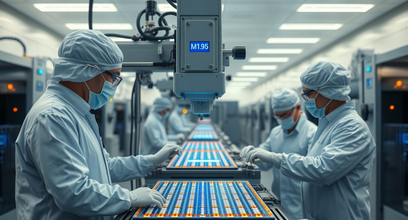
South Korean chipmaker SK Hynix is bringing a massive $29 billion artificial intelligence memory testing facility to Wall Street’s attention, signaling a pivotal moment for the semiconductor industry. The investment, one of the largest ever in memory chip production, underscores the company’s aggressive bet that demand for high-bandwidth memory (HBM) will continue to surge as AI applications expand.
The Scale of the Investment
SK Hynix’s planned expenditure, equivalent to roughly 40 trillion Korean won, is earmarked for a new advanced packaging and testing facility in the United States. This facility is designed specifically for the company’s fifth-generation HBM3E chips, which are critical components in Nvidia’s AI accelerators. The move represents a strategic shift to localize production closer to key customers, reducing supply chain risks and aligning with U.S. semiconductor manufacturing incentives under the CHIPS Act.
Wall Street’s Litmus Test
The announcement arrives as investors closely watch capital expenditure trends in the semiconductor sector. SK Hynix’s decision to seek funding through Wall Street—likely via bond offerings or project financing—will serve as a barometer for institutional confidence in AI-driven memory demand. Analysts note that while HBM sales have skyrocketed, the long-term sustainability of this growth remains a key question. The company’s stock has already priced in significant optimism, and any signs of weakening demand could trigger volatility.
Why This Matters for the AI Ecosystem
SK Hynix controls a dominant share of the HBM market, alongside rival Samsung Electronics. This investment is not just about capacity; it is about technological leadership. The new facility will incorporate advanced testing capabilities that are essential for ensuring the reliability of chips used in large-scale AI training clusters. As AI models grow larger, the need for faster, more power-efficient memory becomes critical. SK Hynix’s bet is that this trend will persist for years, justifying the enormous capital outlay.
Conclusion
SK Hynix’s $29 billion plan is a high-stakes wager on the future of AI infrastructure. The success of this Wall Street test will depend on whether the market believes the current AI boom is a sustainable long-term cycle or a temporary spike. For now, the company is signaling confidence, and the semiconductor industry is watching closely.
FAQs
Q1: What is SK Hynix’s $29 billion investment for?
A: The investment is for a new advanced packaging and testing facility in the U.S., focused on producing high-bandwidth memory (HBM) chips used in AI applications.
Q2: Why is this investment significant for Wall Street?
A: It represents a major capital commitment to AI memory technology, and SK Hynix’s ability to secure funding will test investor confidence in the long-term demand for AI chips.
Q3: How does this affect the broader semiconductor market?
A: It reinforces the trend of chipmakers localizing production near key customers and highlights the strategic importance of HBM technology in the AI supply chain.
Disclaimer: The information provided is not trading advice, Bitcoinworld.co.in holds no liability for any investments made based on the information provided on this page. We strongly recommend independent research and/or consultation with a qualified professional before making any investment decisions.